SPI (Serial Peripheral Interface) protocol is a synchronous serial data link which operates in full duplex mode. It’s got a higher throughput compared to I2C or SMBus and it’s very useful for high speed short-range communications.
The SPI protocol specifies the following signals:
- SCLK — Serial Clock (output from master)
- MOSI/SIMO — Master Output, Slave Input (output from master)
- MISO/SOMI — Master Input, Slave Output (output from slave)
- SS — Slave Select (active low, output from master)
All lines can be shared for every slave device in the bus except the Slave Select signal which has to be different (out of band selection) for each slave.
This is the basic operation depending on the CPOL and CPHA values:
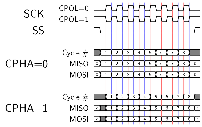
The SPI core I’ve implemented is fixed for Slave and CPOL=0/CPHA=0 modes. This means that the MOSI line will be sampled at every rising edge of the SPI Clock whilst the MISO signal will be set right before this rising edge (actually, on the falling edge) so that it can be properly sampled by the Master.
As the FPGA will have its own clock, we’ll be having two different clock domains since the SPI master signals will be generated externally and they won’t be necessarily synchronized to the FPGA internal clock. Thus, the approach will be sampling all the external signals to get them synchronized and using two shift registers for input and output data.
Source code:
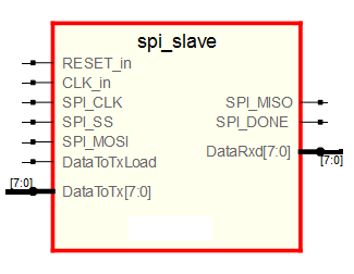
entity spi_slave is
  port (
    RESET_in    : in  std_logic;
    CLK_in      : in  std_logic;
    SPI_CLK     : in std_logic;
    SPI_SS      : in std_logic;
    SPI_MOSI    : in  std_logic;
    SPI_MISO    : out std_logic;
    SPI_DONE    : out std_logic;
    DataToTx    : in std_logic_vector(7 downto 0);
    DataToTxLoad: in std_logic;
    DataRxd     : out std_logic_vector(7 downto 0)
    );
end spi_slave;

architecture Behavioral of spi_slave is

    signal SCLK_latched, SCLK_old : std_logic;
    signal SS_latched, SS_old : std_logic;
    signal MOSI_latched: std_logic;
    signal TxData : std_logic_vector(7 downto 0);
    signal index: natural range 0 to 7;
    signal RxdData : std_logic_vector(7 downto 0);

begin

 --
 -- Sync process
 --

  process(CLK_in, RESET_in)

 begin
    if (RESET_in = '1') then
      RxdData  '0');
      index <= 7;
      TxData  '0');
      SCLK_old <= '0';
      SCLK_latched <= '0';
      SS_old <= '0';
      SS_latched <= '0';
      SPI_DONE <= '0';
      MOSI_latched <= '0';

    elsif( rising_edge(CLK_in) ) then

      SCLK_latched <= SPI_CLK;
      SCLK_old <= SCLK_latched;
      SS_latched <= SPI_SS;
      SS_old <= SS_latched;
      SPI_done <= '0';
      MOSI_latched <= SPI_MOSI;

      if(DataToTxLoad = '1') then
          TxData <= DataToTx;
      end if;

      if (SS_old = '1' and SS_latched = '0') then
          index <= 7;
      end if;

      if( SS_latched = '0' ) then
         if(SCLK_old = '0' and SCLK_latched = '1') then
            RxdData <= RxdData(6 downto 0) & MOSI_latched;
            if(index = 0) then -- cycle ended
               index <= 7;
            else
               index <= index-1;
            end if;
         elsif(SCLK_old = '1' and SCLK_latched = '0') then
            if( index = 7 ) then
               SPI_DONE <= '1';
            end if;
            TxData <= TxData(6 downto 0) & '1';
         end if;
      end if;
     end if;
   end if;
   end process;

   --
   -- Combinational assignments
   --

   SPI_MISO <= TxData(7);
   DataRxd <= RxdData;

end Behavioral;
In order to test this core I wrote a simple testbench wich basically waits for a command from the master and answers it. This will serve as a base for the microcontroller code which will send this same command (0xA0) and wait for the answer (0xA4). This is the simulation view:
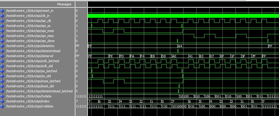
As you can see, when the spi_done signal goes high, the datarxd register is loaded with the value 0xA0. Afterwards, the answer to this command (0xA4) is loaded into the datatoxload register and the MISO line is set to the right bit at every falling edge of the SPI clock signal.
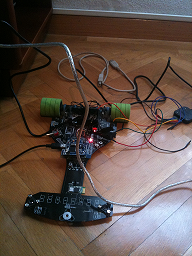
As the simulation looks good, I decided to wire up the FPGA to an LPC2148 microcontroller and test the SPI core for real. The following code will run in the LPC:
void send_fpga_cmd(unsigned char cmd)
{
    unsigned char dummy;
    IO0PIN &= ~(1<<11);    // Select FPGA
    while ( !(SSPSR & 0x02) );
    SSPDR=(unsigned int) cmd;
    while((SSPSR & (1<<4)));
    IO0PIN |= (1<<11);    // deselect FPGA
    dummy = SSPDR;         //flush the RxFIFO

}

unsigned char read_fpga_byte()
{
    unsigned char data;
    SSPDR= 0xFF;         // write dummy data out to gen clock
    while((SSPSR & (1<<4)));
    data = SSPDR;
    return data;
}

while(1)
{
    send_fpga_cmd(0xA0);
    data = read_fpga_byte();
}
I configured the SPI bus to run at 2MHz on the microcontroller. Here you can see the logic analyzer output which shows that the SPI core works as expected.
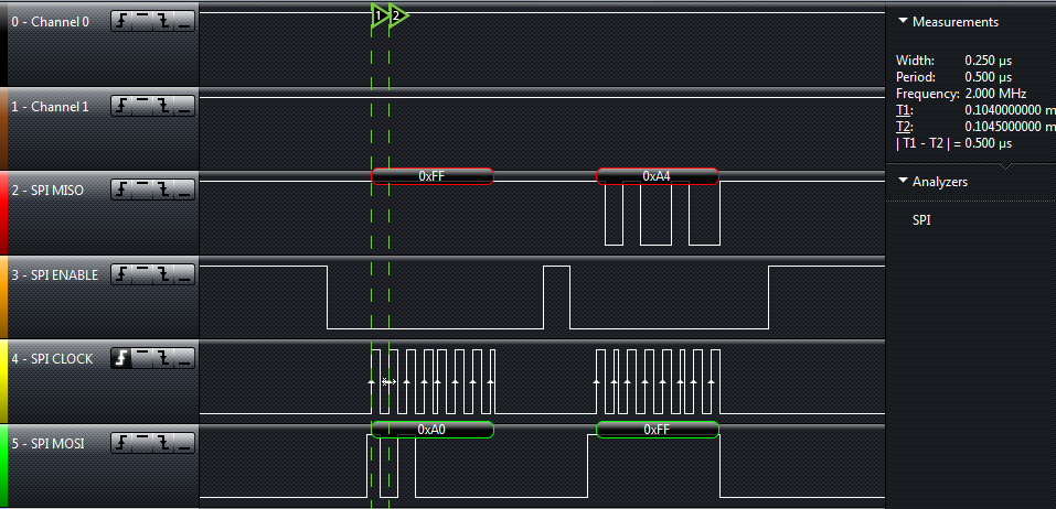
As you can see, the microcontroller sends a ping (0xA0 byte) and the FPGA answers with a response command (0xA4 byte). The SPI clock frequency is exactly 2.000MHz and the behavior is the expected one.
Silvestre FPGA – SPI Test
Daniel